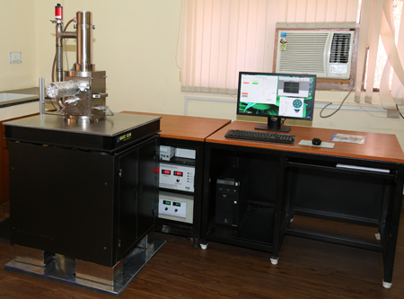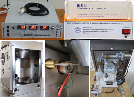

Tungsten filament based Scanning Electron Microscope (SEM) is a scientific investigative instrument that uses a finely focused beam of electrons for microscopic imaging and microanalysis of specimen. It can image specimen with resolution down to 20nm. SEM's accommodativeness of wide range of samples with minimum sample preparation compared to other electron-microscope variants, has rendered it an indispensable tool for imaging and micro-analysis in various disciplines of science including material science, chemistry, geology, pharmacy and forensics. Indigenously developed SEM shall be cost-effective import-substitution for Indian institutions of higher education, research labs and industries etc.
Tungsten filament based Scanning Electron Microscope (SEM) is a scientific investigative instrument that uses a finely focused beam of electrons for microscopic imaging and microanalysis of specimen. It can image specimen with resolution down to 20nm. It is an indispensable tool for imaging and micro-analysis in various disciplines of science including material science, chemistry, geology, pharmacy and forensics. Indigenously developed SEM shall be cost-effective import-substitution for Indian institutions of higher education, research labs and industries etc.
Tungsten filament based Scanning Electron Microscope (SEM) is a scientific investigative instrument that uses a finely focused electron beam for microscopic imaging and microanalysis of specimen. SEM is an indispensable tool for imaging and micro-analysis in various disciplines of science including material science, chemistry, geology, pharmacy, forensics and semiconductor industry. It also finds wide application in mining, metal and steel industry. Indigenously developed SEM shall be cost-effective import-substitution for Indian institutions of higher education, research labs and industries etc. The SEM has imaging resolution of 20nm.
Potential application areas of the SEM are:
SEM has become an indispensable material micro-imaging and micro-characterization tool for disciplines of sciences. SEM shall be cost-effective import-substitution for Indian institutions of higher education, research labs and industries etc. Prompt service and maintenance compared to imported machines. Easily configurable with commercially available Energy Dispersive X-ray Spectroscopy detector for elemental characterization of specimen.
Electron beam emanating from the filament is demagnified and then focused on the specimen by using electromagnetic coils. When the primary beam hits the sample, it ejects electrons from the atoms of the sample, called secondary electrons (SEs). Scanning causes SEs to be generated from all the points hit by the primary beam in the scanned area. The display of intensity (which is proportional to the number of SEs emitted) of each point is visible as the 2-dimensional image.
| Sr. No. | Specification | Value |
|---|---|---|
| 1 | Power supply | 30kV |
| 2 | Vacuum level | 1 × 10⁻⁵ torr |
| 3 | Specimen stage | 5-axis (Motorized) |
| 4 | Magnification | 50x to 1,50,000x |
| 5 | Resolution | 20nm |

